My interest in photography, light and electronics has produced a long standing desire to make digital pinhole camera. In essence I wanted to use a simple photoresistors to create a camera. Obviously such a camera would be slow and produce crude images. So this has been sitting at the back of my brain for a while. Recently my interest was reignited when I saw this example on Hackaday.
My design would use an array of 8 photoresistors aligned in a vertical array. A servo motor would sweep the array from side to side to gather light readings. Why? Using a curved plane for a pinhole reduces some of the distortions. I decided to tackle this project head on.

After prototyping the circuit I knew that would need a compact circuit, with the photoresistors packed closely together and near perfectly aligned. I decided this would be a good time to try creating my own PCBs. Through the IMA Low Res program I had all the tools I needed at NYU.
PCB Design Process
I chose to layout the circuit in Fritzing because I had some familiarity with the breadboard tool of the software and thought it would have a low barrier to entry. After fumbling around for a bit I was able to produce a circuit design.

Later on, I decided to reduce the circuit to just use one array between the photoresistor and ground. More on this later.

The software wasn't too hard to use but I found myself making all of the traces by hand. The auto-trace was completely useless for this.
Milling Time!
With the help of the floor tech Ian, I was able to get the Bantam milling going. Always cool to sit there and watch it do its thing.
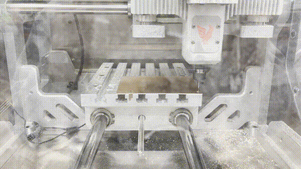
I was able to get a decent board on the second try. I decided to mill out all space outside of the traces, this took longer but I liked how it looked.
Here is a shot of the board in various stages of production.

It wasn't the easiest piece to solder. I found that the foil would burn off easily so I had to be careful. I was able to get a decent result and was ready to work on the programming.
One Resistor Fail!
Remember how I decided to optimize the design early on with one resistor? This was a HUGE mistake. I thought I had got this design working on the breadboard, but I must have made that up. Because when I connected my beautiful custom board to the Arduino and started capturing light readings the numbers were all garbage. The reading for each value was basically the same, even if I had the flashlight pointed directly on a single resistor or if I covered up a single resistor. So this was a huge conceptual flaw that I introduced into the circuit by trying to be too clever.
Starting over I repeated the process with a new design that used a 10k resistor for each photocell. I switched from using photoresistors to phototransistors because I had more of these around and they are faster and more accurate.
Success?
Fast forward a bit and I have my new circuit wired up, the code prototyped, and a camera body for the pinhole.
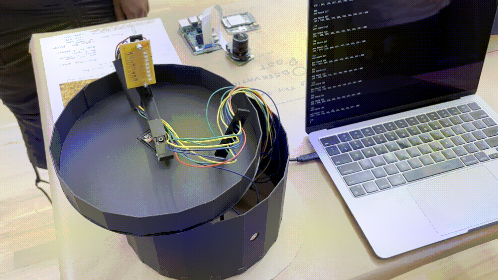
Looks amazing right? Only one thing, two of the phototransistors are giving back readings that are too high and never change.

This was so frustrating and likely something wrong with the soldering of the array or the protoboard I used to hold the Arduino.
So all that work for nothing!
Next Steps
So where do I go from here? Building this prototype taught me a lot about PCB production. The biggest learning, it's great for prototyping but not the best solution. In the future I will likely refine the circuit and send it off to be produced.
Here are some things I plan to do next:
- Prototype More! - I need to work on the turning mechanism and housing. I also need to refine the distance from the pinhole to the sensor path. Making some analog pinholes might be the best way to figure this out!
- Learn Eagle - seems like a better software tool than Fritzing
- Get a board made - I want to use a flexible ribbon for connecting that sensor array to the Arduino. I think the only way to get this made will be to have the board produced by a company. I was unable to mill headers on my prototypes because the tracing was too tight. The added benefit is I'll be able to get a more compact design for the PCB.